¶ Current Design (V2.0)
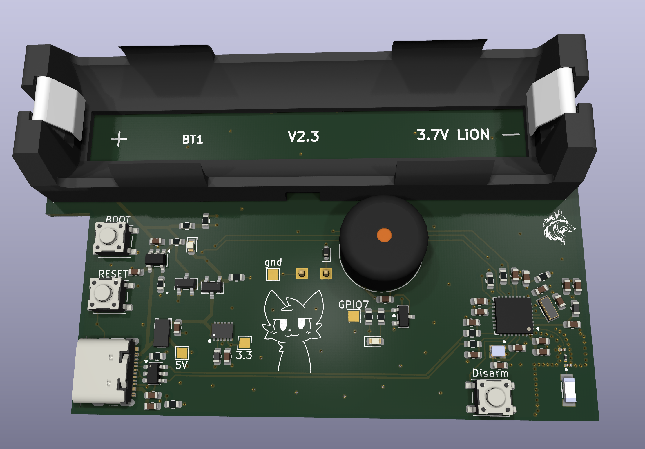
¶ Introduction
In 2025, I started building my first-ever PCB. My parents had water damage in their basement, and we noticed it too late because there was no water detector.
That’s why I decided to build one based on the ESP32, which can report water leaks over Wi-Fi and connect to a Node-RED instance to alarm my parents in time.
But simply putting a finished ESP32 dev board in the basement wasn't what I wanted to do. The power consumption on these boards is quite high, and I had been wanting to design my own PCB for a few months anyway, so I took this as the perfect opportunity.
However, using a pre-assembled ESP32 module on the PCB—as most tutorials and people online recommended felt too easy. I had never designed a PCB before and thought: "Nah, putting a pre-built board onto another board requires no skill and is boring."
That’s why I wanted to make it from scratch using the bare ESP32-C3 chip, along with custom power management and an antenna. I also used two crystals: the main 40MHz clock for the ESP and a 32.768kHz crystal for the RTC timer. This allows the chip to save CPU cycles during deep sleep, which gives a few months extra battery lifetime.
I completely overestimated myself with that project and learned that it is not as easy as it seems. But in the end, it was a great way to get into PCB design. If I had just used a finished module, I wouldn't have learned nearly as much.
¶ V1
I have two iterations of the board. When I designed the first one, I watched many YouTube videos for tips, tricks, and the "dos and don'ts" of PCB design. I looked at the most common beginner mistakes and then started on the schematics.
With the help of AI, mainly Gemini, I worked out the best parts for my project.
The ESP32-C3 was my favorite from the start because I knew it was low-power and I didn't need many GPIO pins. Gemini confirmed my choice. I looked up a few voltage regulators and Gemini suggested this one because it can output enough power but has an extremely low quiescent current (IQ) while the ESP is in deep sleep.
Next, I searched for an LED and a loud piezo module. After gathering all the components, I placed them on my schematic and connected them as the datasheets and tutorials instructed. At that point, I thought: "This is so easy."
Then I had to arrange the parts on the PCB and route everything, which was quite challenging because there were many components and I didn't yet know how to use KiCad correctly.
Eventually, I finished it and ordered the boards. Since I didn't know any experts in the field, I had to rely entirely on myself and online resources.
The PCBs arrived two weeks later, and I was really hyped. I bought a hot plate, assembled the complete PCB at once, and connected it to my computer via USB. I was excited to see it connect, but... it didn't show up.
I spent the next few days troubleshooting and found several issues.
¶ Problems
One major flaw in my design was that I misinterpreted the datasheet:

This is an excerpt of the pin descriptions. I read the first sentence and thought it was irrelevant since I don't utilize the LOAD pin. I took a quick look at the second sentence, which gives instructions on how to configure the pin, but I skipped the last sentence because I didn't see any importance in it. The last sentence states that the pin must be connected. This means that if it floats, the whole chip is disabled and won't output the 3.3V I needed. It took a while to figure this out because I didn't include any test pads. I had heard they were important, but I was so sure my schematic was perfect that I didn't add any.
The next problem was that I put a capacitor in series with the power chip. I misinterpreted the datasheet and didn't know at the time that decoupling caps are never in series with the power line, but always go to GND.
I also used some diodes with a size of 0.2mm x 0.5mm (0201). I was used to 0603 components looking quite big in the 3D view of my PCB software, so I was confident they would be okay for hand soldering. They were not. I actually got them to work, but it was a massive hassle to find the correct orientation under a microscope and solder them properly so I ended up bridging them in my next attempts on the other pcbs.
For the battery, I chose a 3.7V Li-ion cell because they have lower self-discharge than normal AAA batteries. I asked an AI for the dimensions, and it said they were the same as a normal AA battery. So, I ordered an AA battery holder, only to discover that Li-ion cells are quite a bit larger and don't fit.
¶ Upgrades in V2
After soldering all five PCBs I ordered from JLCPCB, I knew I had to redesign the board, fix the errors, and order again. I also found another problem while double checking my design: I had placed a capacitor in series with my clock signal to the ESP. After fixing these issues and adding test pads, I felt confident again, but this time, I asked for a review on Reddit first. One person was extremely helpful and explained why the design was still basically non-functional.
Because of that feedback, I connected the crystal correctly to GND, improved the loop areas for the decoupling capacitors, and moved all caps and the crystal much closer to the ESP chip. I also shortened the antenna feedline, added a proper differential pair for the USB lines, and added optional capacitors to the USB data lines and ESD protection for the USB port and the water-sensing GPIO. I improved the trace thickness for correct impedance on the USB and Wi-Fi antenna lines, corrected the net labels in KiCad, and added a MOSFET to cut off the battery when USB is connected instead of relying on diodes. Finally, I added vias to the ESP32’s thermal pad and used a smaller footprint for the antenna matching circuit.
During the redesign, I also added a charging circuit, because it would be a waste not to have one. I ordered the PCB without major further changes, as most remaining comments were just about aestheticsa and disencouraging me from tring to not use a finished module.
¶ Problems in V2
When the new PCBs arrived, I started by populating only the power circuit. Testing with a USB-A to USB-C cable worked perfectly: I got 5V from USB and 3.3V from my regulator on the first try! I was happy and continued soldering the processor, the crystals, and the other core components.
However, when I tried to connect it with a USB-C to USB-C cable, I didn't get a signal. I was bamboozled and tried everything: changing the pull-up/down resistors on the strapping pins, trying different cables, and different computers. Nothing helped. I didn't even get power with a C-to-C cable, which was irritating because A-to-C worked fine.
To dig deeper, I connected the board to my Arch Linux machine. When I ran lsblk, the command froze and only resumed once I unplugged the board. This only happened if the USB-C plug was oriented one way; the other side did nothing. After digging into the USB protocol logs, I found that the board was recognized as a device but failed to negotiate IDs or speed. I eventually cut open a USB-C cable to measure the connections.
To my surprise, they didn't match. The CC pins weren't connected at all, which is why USB-C to USB-C power negotiation failed (USB-A to C just pushes 5V regardless). I discovered that while the USB-C standard is documented in a massive PDF, the physical pinout of the connectors themselves is not standardized across all manufacturers. I had ordered the wrong USB-C ports for my footprint. Luckily, I had a spare connector in one of my parts bin that fit. After replacing it, the controller was finally recognized as an ESP board!
I thought I was in the clear, but then I tried to flash the ESP and got a "Flash read/write error." I was devastated. I spent an hour digging through the datasheet, checking every power pin, and even connecting a 3.3V lab power supply because ChatGPT suggested my regulator might not give enough current for flash writes. Nothing helped. Then it hit me: Did I order the wrong chip? I checked my Mouser order and realized I had ordered the ESP32-C3 variant without built-in flash.
After a major facepalm, I wanted to order the correct one, but Mouser has €25 shipping for a €2 product. I tried ordering from AliExpress instead to save on shipping. As soon as i unpacked them and wanted to start solder them i realized that it was a mistake. I ordered five esp32-c3 chips; the ones from Mouser had clean, sharp edges, but 3 of the 5 AliExpress ones looked rough and damaged. I tried them anyway but none of them worked. Two of the 5 actually looked fine and conneted to the computer. But one didnt recognized the flash and the other was not able to get into flash mode. Maybe they were damaged, or locked somehow but in the end they none of them worked at all.
Because i didnt want to buy the esp32 chip somewehere else and wait for it to arrive, I desoldered one controller from a previous bought esp32-c3 dev board which i hadnt used yet. It worked instantly and i got a blinking led.
¶ Problems in V2
There is still an issue in my second revision. I soldered the components for the charging circuit and measured them because a MOSFET, which wasn’t supposed to get warm, got really hot. I was shocked to see that the USB bus voltage drops to around 4.3V and charges directly into the Li-ion battery. I immediately disconnected the circuit and looked into it. That’s when I discovered MOSFETs aren't "perfect" on/off switches; they always allow current to flow from Source to Drain via the body diode, which caused the voltage drop and the heating.
The antenna line is still untested, but I expect I may have miscalculated the trace width. I will start measuring it soon to be sure.
¶ V3
In this revision, I added another MOSFET to the charging circuit to create a proper back-to-back MOSFET circuit. I could also just add a diode, but I don’t want any voltage drop between my battery and the power IC.
I also fine tuned the antenna even more. I measured the signal reflection with my LiteVNA but i couldnt reach good values even with theoretical good component values in the pi matching network. After I looked into it i discoverd i did not choose the right track width for the selected stack up in the ordering process.
¶ Measuring with the liteVNA
After the new and corrected PCB arrived, I tested the signal reflections again. At first I was devastated, because after bridging the pi network with a 0 Ω resistor the results looked like this:
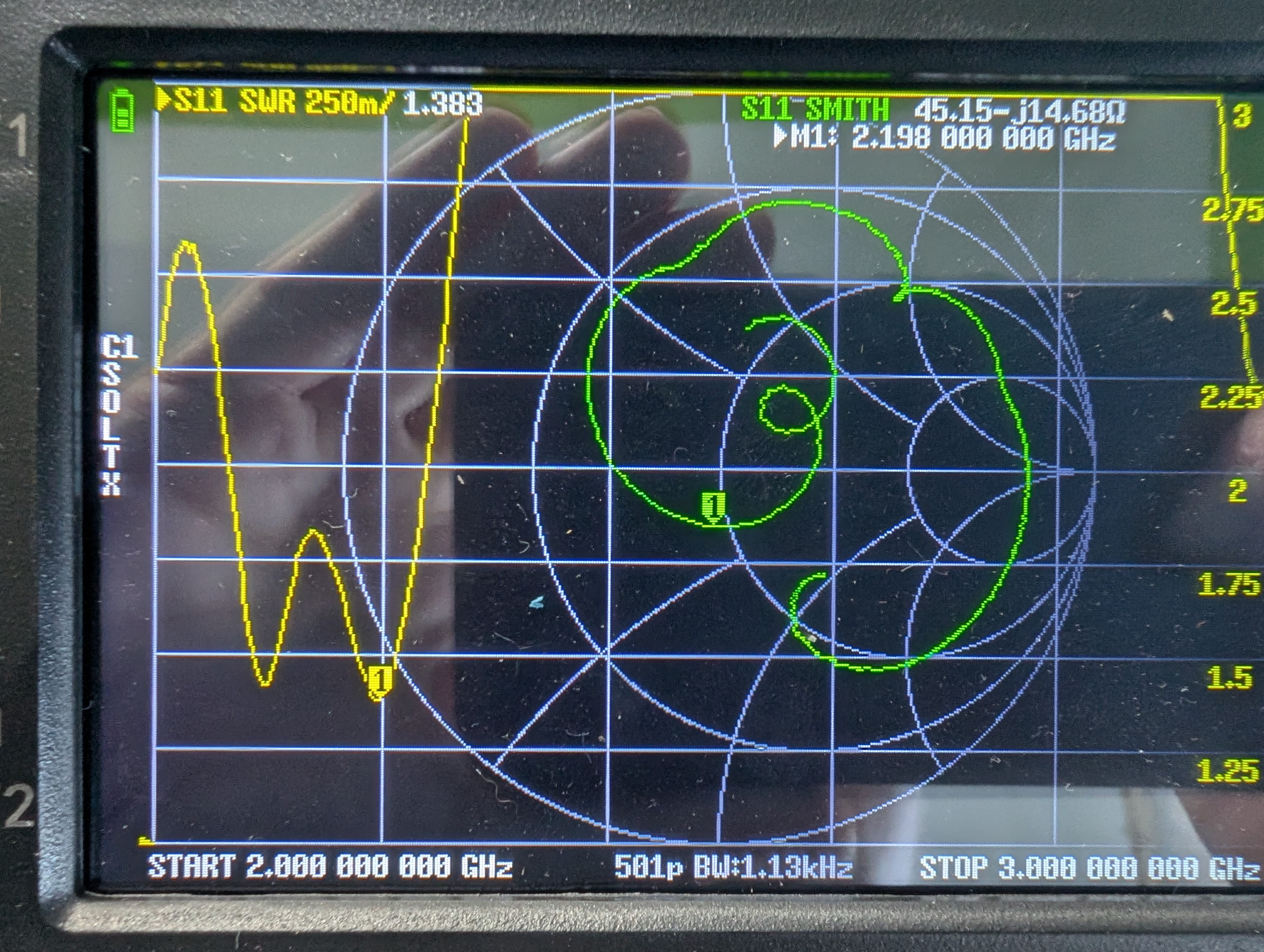
The antenna's self-resonance sat way too low for WiFi, which operates in the 2.4 GHz ISM band (2.400–2.4835 GHz). A detuning of that magnitude isn't something a pi matching network can realistically pull back into band. On top of that, the trace on the Smith chart didn't behave like a normal antenna should — not even a badly mismatched one. After digging through my design files again and comparing it to the antenna datasheet, I couldn't find any errors in my design. After asking AI it tried to tell me my design is completly wrong but the datasheets said otherwise and then the AI said I am correct...
Then it hit me: maybe I hadn't only connected the antenna feedline to the VNA, but had accidentally bridged an adjacent pad as well, shorting part of the network and corrupting the measurement. I confirmed the theory shortly after and cleaned up the connection. With the VNA now seeing only the antenna and its feedline, I got this:
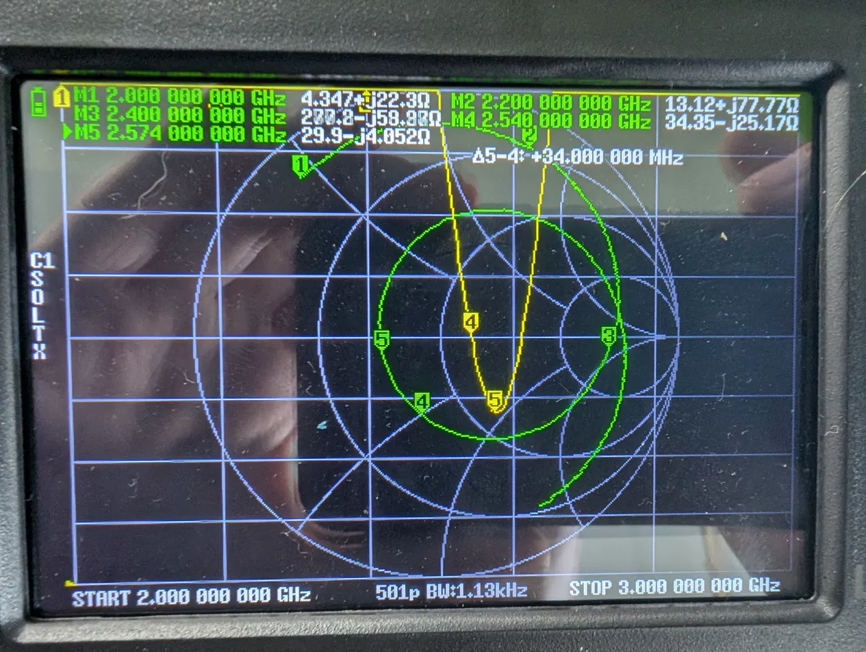
Much more promising. From here I only had to match the pi network: pull the resonance down slightly into the band and kill the remaining reflection.
A quick note on what the measurement actually shows: the parameter being plotted is S11, the reflection coefficient at the antenna port. On the linear plot it appears as VSWR (voltage standing wave ratio), where 1.0 is a perfect match and everything above it means part of the incident power is being reflected back instead of radiated. The Smith chart is the same data mapped onto a complex-impedance plane: the center point is a perfect 50 Ω match, and how far the trace sits from center tells you the mismatch. The frequency where the trace crosses the real axis (imaginary part ≈ 0) is the antenna's self-resonance.
(AI generated info while i figured everything out)
I started with the series inductor (L1). After sweeping through a few values, I learned that larger inductances shift the resonance further down. 2.2 nH turned out to be the sweet spot with 2.458GHz at the bottom:
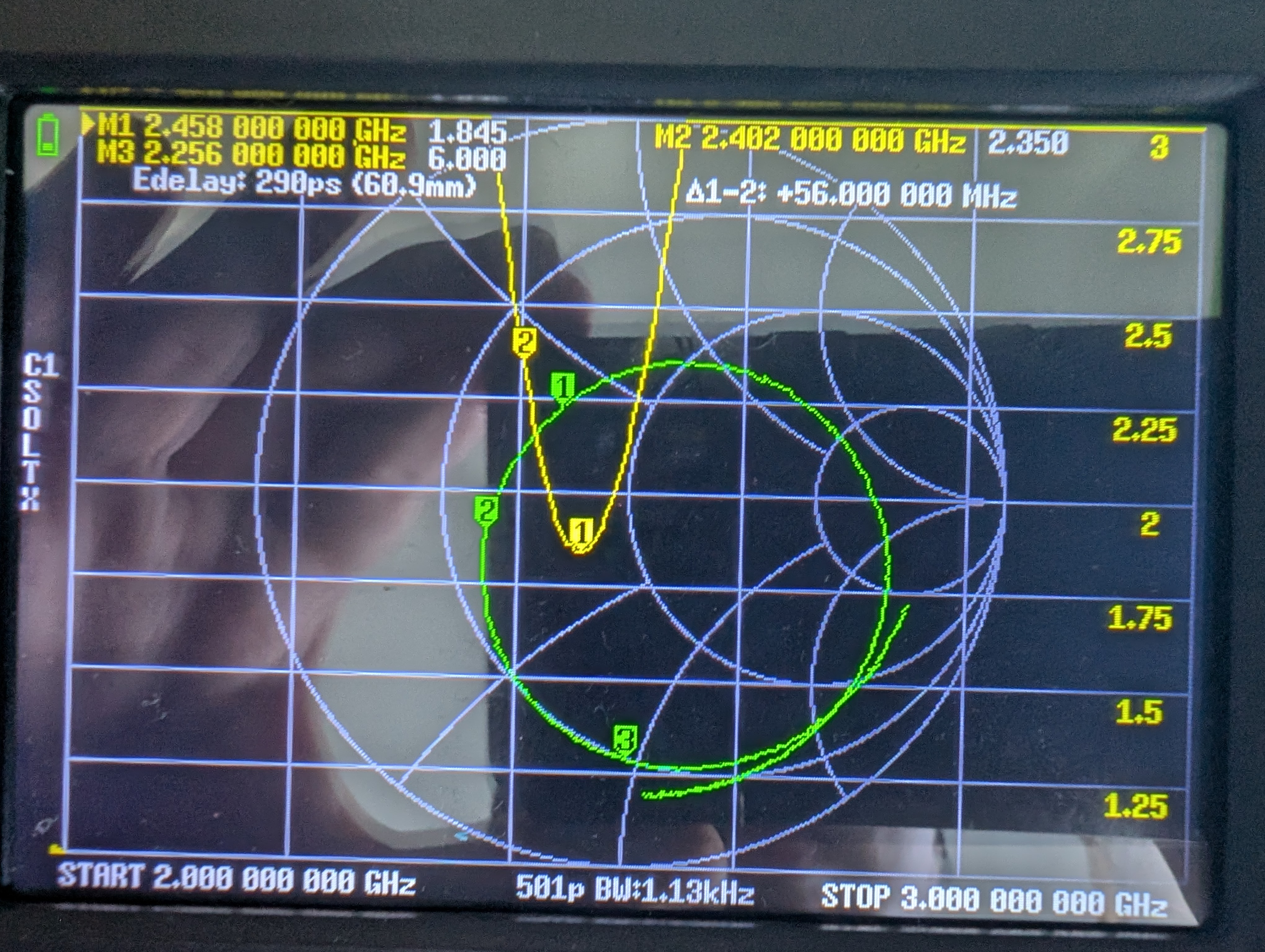
At these frequencies small value changes make a big difference. For comparison, bumping the inductor up to 2.7 nH already drags the resonance too far down. 2.354GHz is not in the wifi band anymore:
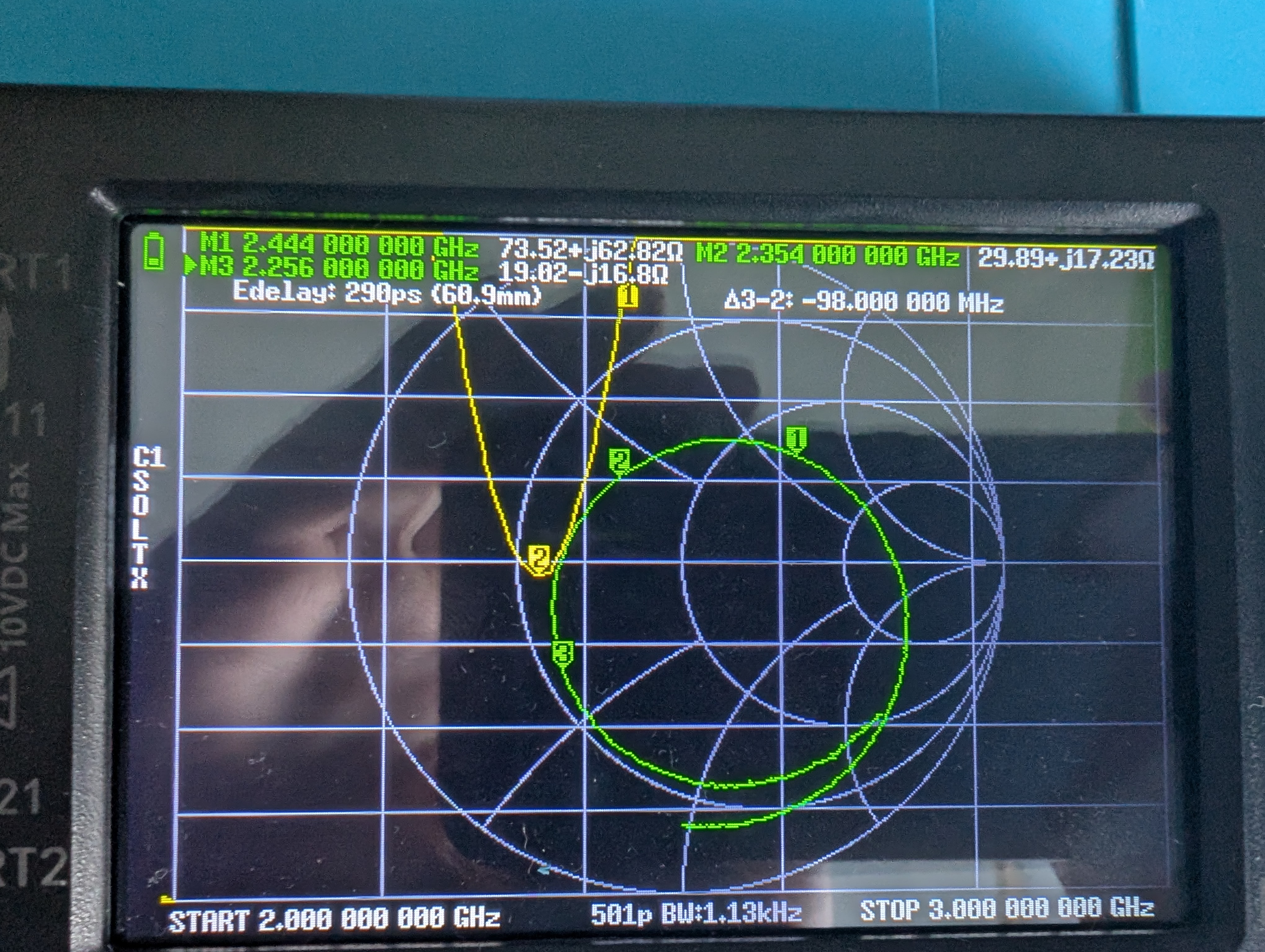
Why such small values swing the result so hard: at 2.4 GHz the wavelength is only ~12.5 cm, so even a fraction of a nanohenry represents a meaningful reactance (X = 2πfL). A 0.5 nH change in the series inductor already shifts the reactance by several ohms at this frequency, which is enough to move the resonance by tens of MHz.
(AI generated info while i figured everything out)
With the resonance sitting right, the last step was reducing the return loss, which meant adding a small shunt capacitor to the network. From earlier attempts I already knew that oversized capacitors throw the match off almost instantly, so I started with the smallest value I had on hand — 0.5 pF — and it was good enough right away:
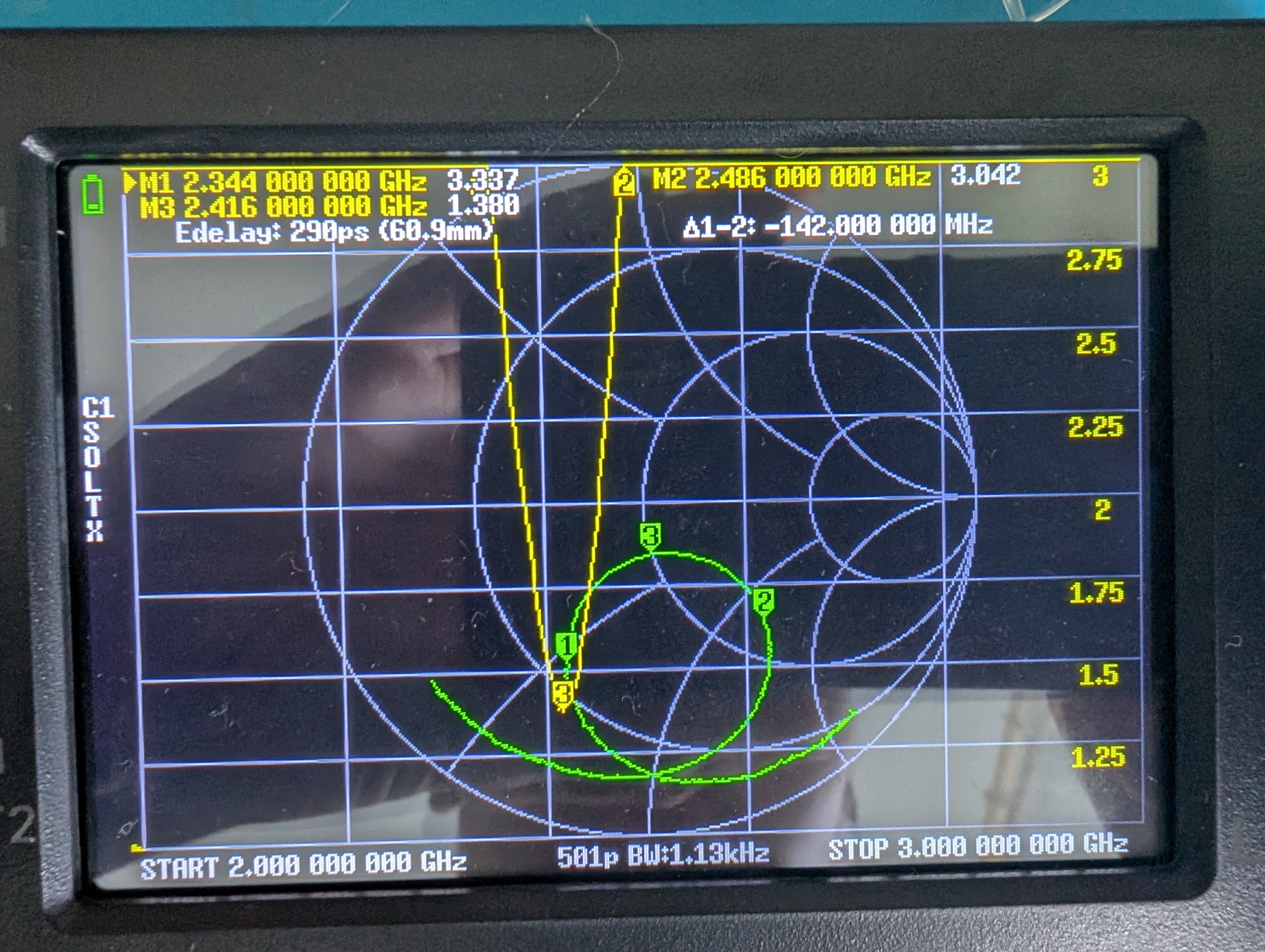
One thing worth knowing for a chip antenna like this: its radiation resistance is low (measured around 17 Ω at resonance), which means the matching network has to transform quite far up to 50 Ω. This gives the match a relatively high loaded Q, and high Q inherently means narrow bandwidth — the classic Bode-Fano tradeoff. That's why the dip is sharp rather than broad. For a device that talks on a single fixed WiFi channel this is a non-issue, but it explains why chasing an even deeper match would only make the usable bandwidth narrower.
(AI generated info while i figured everything out)
With that I got my first ever fine tuned antenna done! :3